
A. Barr
J. Carter
Cambridge University
A.A. Carter
Queen Mary, University of London, UK
J.C. Hill
Cavendish Laboratory
L. Eklund
CERN
Z. Dolezal
V. Vorobel
Charles University, Prague
T. Horazdovsky
I. Stekl
Czech Technical University Prague
P. Kodys
Freiburg University, Germany
P.W. Phillips
Rutherford Appleton Laboratory, Didcot, UK
G. Moorhead
University of Melbourne
Y. Unno
KEK, Tsukuba, Japan
G. Llosa Llacer
M.A. Vos
IFIC - University of Valencia
This document aims to describe the "Valencia" analysis of the 2000 SCT test beams in H8, with a special focus on the August run.
Impatient readers can jump to the chapter that has their special interest.
The introduction describes what data were taken and why.
The offline & alignment chapter describes the steps to go from raw data to DSTs including the alignment and track reconstruction.
The analysis section briefly describes the methodology of the analysis.
Finally, the latest results are summarized.
DISCLAIMER:These results can freely be used in presentations, as long as this is previously discussed with the authors. The same results were summarized in a note (download a draft here). It is advised to refer to the note, rather than to the web page.
NOTE:A number of corrections had to be applied to obtain real values from the nominal ones. The threshold points taken have to be corrected on a plane-by-plane basis using the in-situ calibration (run 1429). The charge obtained have to be scaled to correct for detector thickness. The bias voltages have to be corrected for the voltage drop in the bias resistor. This has not been done for all plots, partly to keep the connection to runs clear and partly for practical reasons (binning, markers, etc.). I hope the captions are clear as to what corrections have been applied. If not, please let me know.
All figures are JPG to facilitate viewing, but the PostScript originals are also available. In case people want the print this document, they are advised to print the PostScript figures.
The main aim of the June and August test beams was to study the behaviour of irradiated detectors and electronics in circumstances similar to those expected in the final experiment. To this end, the runs were organized in nested scans of threshold, bias voltage, incidence angle and magnetic field strength. A total of over a 1000 runs of 5000 events each were taken. In both cases the data can be diagrammed as below:
2 B=0, B=1.56 T
5 incidence angle
5 bias voltage
12 threshold
These data are complemented by noise runs (taken in situ, but with no beam) and local calibration runs (temperature and grounding in the box might invalidate calibrations taken previously in the laboratory)
In the August run 9 SCT prototypes were read out. Among these three barrel modules with irradiated detectors, 1 fully irradiated barrel module, three non-irradiated barrel modules and three non-irradiated forward modules. The list below summarizes the most important properties for all modules.
K3112 KEK <100> detectors
K3113 KEK Irradiated <100>
RLT5 UK 325 um detectors
RLT4 UK Fully irradiated module with 325 um detectors
RLK6 UK Reference module
RLT9 UK Irradiated detectors
RLT10 UK Irradiated <100> detectors
VAL1 Val. Forward module
FRK152 FR Forward module
FRK153 FR Forward module
SCAND1 Scand. <100> detectors
Anch2 Melb. Anchor
Anch3 Melb. Anchor
The list supposes modules to be unirradiated barrel modules, with 285 um <111> detectors. Anything that differs is indicated.
In June, 8 DUTs were tested, among which RLT9, with irradiated detectors. In the May test beam the SPS was operated with an LHC-like 25 ns bunch structure. This allows the study of subtle timing effects in a situation very similar to the final ATLAS environment. Results from these two beam periods have been presented in the September SCT week. This report will concentrate on August results.
Apart from the devices under test a beam telescope - consisting of 2 times 4 planes of (slow) analog Silicon Strip detectors - was read out, as well as a TDC, measuring the relative phase of the bunch with respect to the 40 MHz system clock. Further, a number of SCT prototypes is used as anchor (do not follow any scan) or reference module (follows incidence angle scan).
The raw data are processed offline into DSTs. These present the binary data in a more accessible format (ROOT Tree) and provide reconstructed tracks. Together with the internal alignment information, the tracks can be extrapolated to the modules under study. More information, skeleton analysis macros and some hints on getting started can be found on the offline pages
The telescope is used to reconstruct the tracks of the beam particles. These tracks can then be extrapolated to the modules under investigation. Thus, it is necessary to accurately know the relative position of the analog modules making up the telescope and the DUTs. This can be achieved by using the beam tracks to carry out an alignment for all relevant beam periods (after each change of the incidence angle or magnetic field). In the Valencia alignment five parameters are optimised, thus allowing for all rotational and translational degrees of freedom. After the alignment, tracks can be reconstructed for all runs with an accuracy of less than 10 microns. (alignment files to be found http://ific.uv.es/sct/tb00/align/)
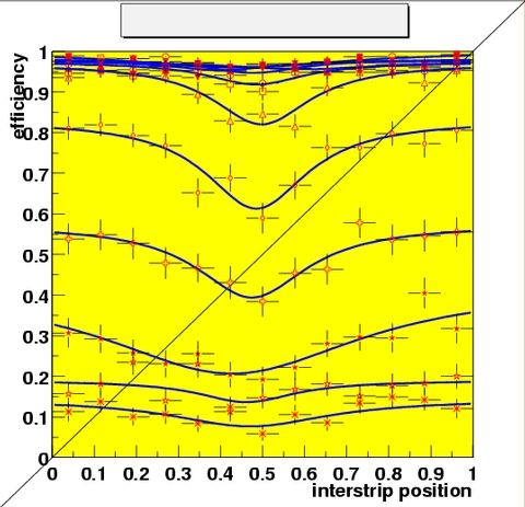
Residuals for one and two hit clusters (leftmost), efficiency as a function of interstrip position of the track for various thresholds, multiplicity of the efficient cluster as a function of the interstrip position of the track(rightmost). Get PostScript 1 23
These images demonstrate the possibility to resolve effects at a scale of roughly 10 microns (for comparison: the pitch of the detectors is 80 microns). The residuals measure the spatial resolution of the binary modules (leftmost figure). The charge sharing in the region between two strips is seen to lead to an increase in the fraction of two-strip clusters (middle figure), which is reflected in a lower efficiency in the intermediate thresholds (rightmost figure).
The final resolution of the track extrapolation using the telescope depends on a couple of cuts. A critical parameter is the minimum number of space points that define a track. Unfortunately, the telescope planes show quite some inefficient regions (especially in some June runs). In order to obtain enough statistics, tracks with only three points had to be accepted. Similarly, the maximum distance to the track had to be kept rather loose. Thus, out of 5000 one obtains around 4000 events with one reconstructed track with good enough spatial resolution for the efficiency analysis. Alternatively, low quality tracks (the Chi-squared of the fit is available in the DST) can be rejected, leading to a smaller, high spatial resolution sample.
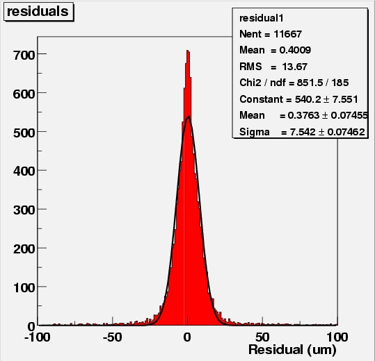
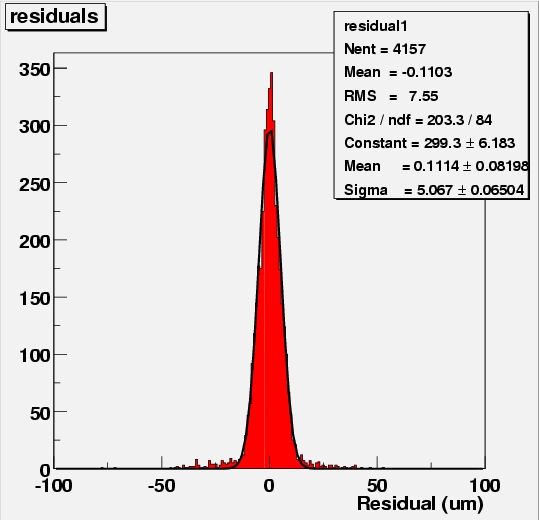

The residuals of telescope plane 0-x for three chi-squared cuts (none in the leftmost figure, 0.003 in the middle and 0.0005 in the rightmost figure). Get PostScript 1 2 3
The residuals of one of
the telescope planes give an idea of how the Chi-squared cut affects
the track extrapolation resolution and the statistics. As the same
telescope plane is used in the fit to determine the track in the
first place, the residuals do not measure the resolution (at least
not in an unbiased way). However, they can be used as a tool to
determine the optimum value of the chi-squared fit. Shown are plots
for no cut (leftmost), a loose cut (middle) and a very strict cut
maintaining only 10 % of the events (rightmost).
|
Chi-squared |
divergence |
spatial resolution (um) |
accepted events (%) |
|
- |
- |
7.5 |
78 |
|
0.1 |
0.02 |
7.0 |
65 |
|
0.1 |
0.002 |
6.9 |
62 |
|
0.03 |
0.002 |
5.1 |
27 |
|
0.01 |
0.002 |
3.4 |
9.7 |
|
0.005 |
0.002 |
2.6 |
4.7 |
Spatial resolution and number of accepted events for different values of the Chi-squared and divergence cuts.
The relation between the Chi-squared cut value, the resolution of the track extrapolation and the statistics retained is clear from the table. The divergence cut can be used to get rid of some badly reconstructed tracks (in the tails of the residuals). Then, lowering the Chi-squared cut value strongly improves the track quality, but - unfortunately - also greatly reduces the statistics.
All the test beam data have been processed into DSTs and are available on the High Performance Storage System (hpss/cern.ch/atlas/testbeam/sct/2000/dst/). Apart from the reconstructed tracks, these contain the trigger phase information measured by a TDC, a number of flags and counters and all data from the binary modules. The data (taken in ANYHIT compression mode) has been reclustered to get independent clusters of adjacent hits in each time bin.
The performance of the DUTs is evaluated by measuring their position measurement of the beam tracks with the positions obtained from the extrapolation of the telescope information (knowing the relative alignment of all devices). Thus, an "efficient event" is defined as an event where a binary hit is found close to the extrapolated track position. Similarly, the spatial resolution can then be measured by calculating the residuals.
This section will describe the cuts used for this analysis and their motivation in some detail.
For the results presented later on in this document a loose cut on track quality (chi-squared < 0.2 and divergence < 0.004) has been used, retaining as much statistics as possible for the determination of efficiency and noise. Only for plots that depend strongly on the spatial resolution (residuals, interstrip position) the cut has been tightened down slightly (chi-squared < 0.05 and divergence < 0.0001).
With these loose track cuts, a rather wide efficient region has been used. All events where a hit is found within 100 micron from the extrapolated track position are considered efficient. Any hits found more than 2 mm away from the track are considered due to noise.
The SPS beam available for SCT beam tests is asynchronous, ie beam particles arrive randomly with respect to the system clock. Therefore, the delay between the beam trigger signal and the next rising edge of the clock is measured using a TDC.
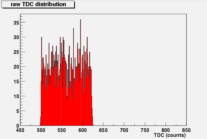
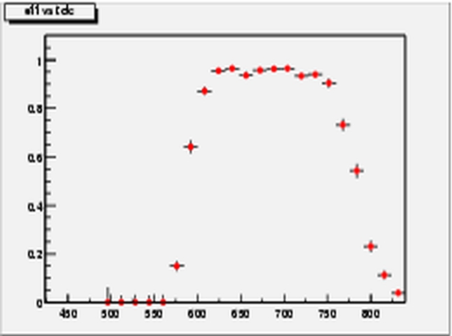
Raw TDC distribution (leftmost figure) and efficiency versus TDC, combined for three time bins (rightmost figure). Get PostScript 1 2
The raw TDC distribution is random in a 25 ns range (leftmost figure, the counts correspond to 0.2 ns). The binary modules provide information from the clock cycles before and after the triggered one. This information can be used to determine the efficiency as a function of trigger time throughout a 75 ns range (rightmost figure, the central time bin corresponds to the raw TDC + 25 ns, that is the interval <500,625>).
Conventionally, a cut was placed on the TDC value, keeping only the "plateau". Alternatively, one can choose to consider an event efficient whenever one of the three time bins was so. The results presented here were obtained using the latter approach.
The noise occupancy was determined per time bin: all noise hits were added and then divided by 3**. Thus, the effect of non-reconstructed tracks mimicking noise hits is reduced.
The ABCD2T chips had very non-linear trim DACs in some of its channels (a problem solved in the ABCD3T). This resulted in a number of non-trimmable and thus unusable channels, especially after irradiation. Further, a couple of channels are always lost due to bonding problems, dead strips on the detector etc. In order to be able to do detailed studies, these have to be masked out. In the analysis these channels are treated in the following way:
Any event that has its track pointing to a bad channel or one of its inmediate neighbours is rejected
Any hits in bad channels or their inmediate neighbours are not counted (of course the number of channels in the noise occupancy is corrected).
The bad channel lists used for this analysis are the sum of the channels masked on the chips by the module responsibles and those found by a routine fitting the hitmap of various runs and rejecting deviating channels.
|
Module |
K3112 |
K3113 |
RLT4 |
RLT5 |
RLT9 |
RLT10 |
VAL1 |
SCAND1 |
FRK153 |
FRK152 |
|
# bad channels |
94 |
126 |
279 |
19 |
201 |
229 |
38 |
277 |
147 |
93 |
The number of bad channels in each module, including channels masked by module responsibles and those found by a bad-channel finding routine.
These numbers of bad channels may seem a bit exaggerated. A "bad" channel is certainly a quite subjective notion. Our criterion in determining the optimum value for all cuts has been that the measured efficiency should approach the ideal efficiency (as obtained with a very strict cut) to within 1%.
This section tries to summarize all available results. Due to the large amount of data it has often been necessary to show plots for only one or two modules or summarize a whole range of plots in one. Mostly, the details do exist in PostScript or can be generated quite easily from the summary Ntuple.
The two most important benchmarks for the SCT are the detection efficiency and the noise occupancy at the operational threshold (envisaged to be 1fC). The methodology has been discussed in the analysis section. S-curves and noise occupancies at the same thresholds have been plotted for all runs and modules. A sample plot is shown below:
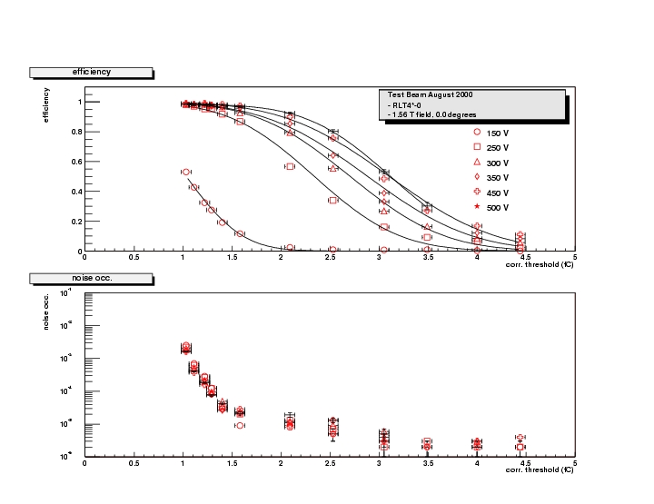
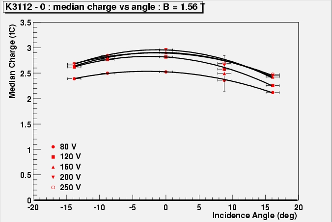
Efficiency, d(eff)/d(thr), and noise as a function of threshold for RLT4 in a 1.56 T magnetic field, perpendicular incidence. PostScript files for all modules
The maximum efficiency approaches 99 % for all modules at 1 fC threshold, provided the bias voltage is high enough for the irradiated modules (higher than 350 V). The first plot presents efficiency versus threshold (S-curve), fit with an error function. The fit generally slightly underestimates the 50 % charge, as the error function can not incorporate the Landau tail of the charge distribution. All median charges quoted further on, will always be the outcome of the error function fit.
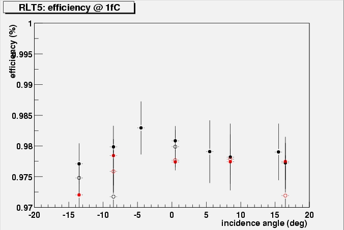

Efficiency at 1.1/1.2 fC for RLT5(left) and RLT4(right). As these modules have thicker detectors, the efficiency is determined at (325/285) fC. Results are shown for different angles, voltages and fields (red = 1.56 T, black = 0 T - full circles at highest voltage 250/450 V, open circles at intermediate voltage 120/300V). RLT4 is an irradiated module . Thresholds are approximate (according to recalibration 1429). Get PostScript files for all modules

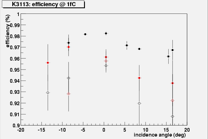
Efficiency at 1 fC for K3112(left) and K3113(right). Measured at different angles, voltages and fields (red = 1.56 T, black = 0 T - full circles at highest voltage 250/450 V, open circles at intermediate voltage 120/300V)
The noise occupancy reaches a plateau at around 10-5. These hits are due to badly reconstructed tracks, incorrectly marked as noise hits (the acceptance of the telescope is smaller than that of the binary modules and it is far from fully efficient). As soon as the noise occupancy starts to rise, however, the value is completely due to real noise, as can be seen from a comparison with the noise occupancies obtained from special noise runs.
Unfortunately, no lower threshold runs were taken for the barrel modules.
The noise occupancy is easier to determine in dedicated noise runs. The tail due to non-reconstructed tracks disappears. The non-irradiated barrel modules have empty plots as the noise level at 1 fC is lower than 10-6!!! The table below lists the noise occupancy evaluated from a Gaussian fit of the plots. Errors are not listed, as they depend critically on the calibration.
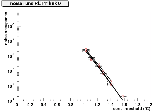
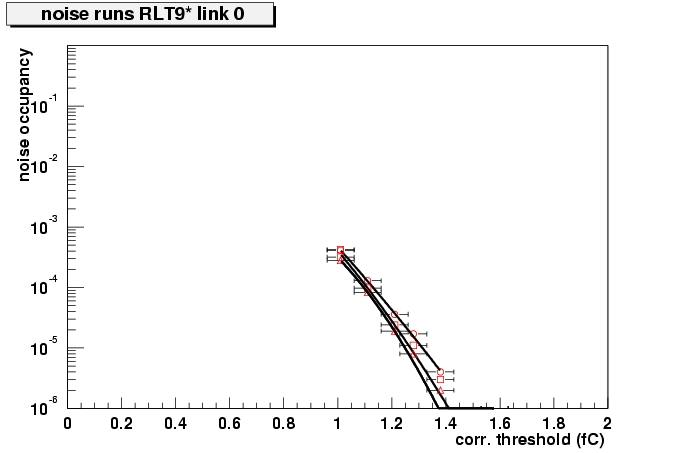
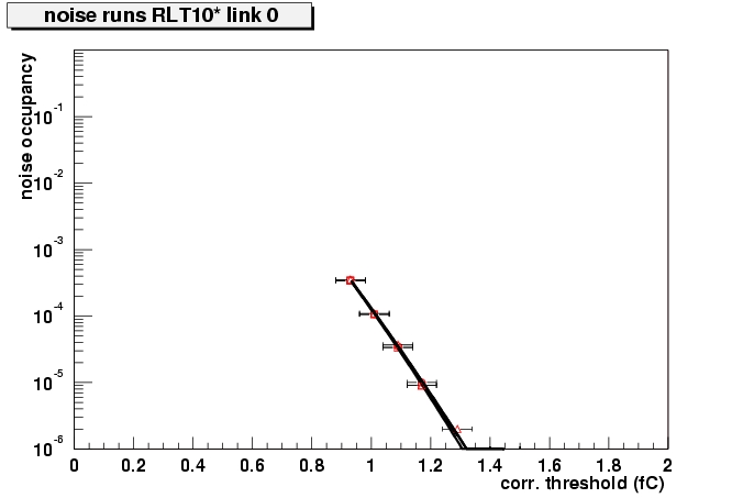
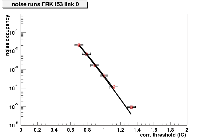
Noise occupancy as obtained from the noise runs for 4 modules. The circles are from the run at lowest voltage (120/250), squares from (200/350) and triangles from (250/450). Get PostScript files for all modules.
|
Module |
occ(1fC) 250/450V |
occ(1fC) 200/350V |
occ(1fC) 120/250V |
|
K3112-0 |
<10-5 |
<10-5 |
<10-5 |
|
K3112-1 |
<10-5 |
<10-5 |
<10-5 |
|
K3113-0 |
<10-5 |
<10-5 |
<10-5 |
|
K3113-1 |
<10-5 |
<10-5 |
<10-5 |
|
RLT4-0 |
0.0038 |
0.0037 |
0.0029 |
|
RLT4-1 |
0.0089 |
0.0084 |
0.0077 |
|
RLT5-0 |
<10-5 |
<10-5 |
<10-5 |
|
RLT5-1 |
0.000101 |
0.000063 |
0.000055 |
|
RLT9-0 |
0.000465 |
0.000402 |
0.000313 |
|
RLT10-0 |
0.000127 |
0.000125 |
0.000131 |
|
RLT10-1 |
0.000005 |
0.000005 |
0.000005 |
|
SCAND1-0 |
0.000003 |
0.000002 |
0.000002 |
|
SCAND1-1 |
<10-5 |
<10-5 |
<10-5 |
|
FRK153-0 |
0.000482 |
0.000424 |
0.000402 |
|
FRK153-1 |
0.000207 |
0.000215 |
0.000196 |
|
FRK152-0 |
0.000647 |
0.000532 |
0.000568 |
|
FRK152-1 |
0.000402 |
0.000323 |
0.000287 |
The noise occupancy at 1 fC as measured in the noise runs, for all modules and 3 bias voltages.
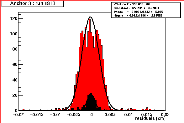
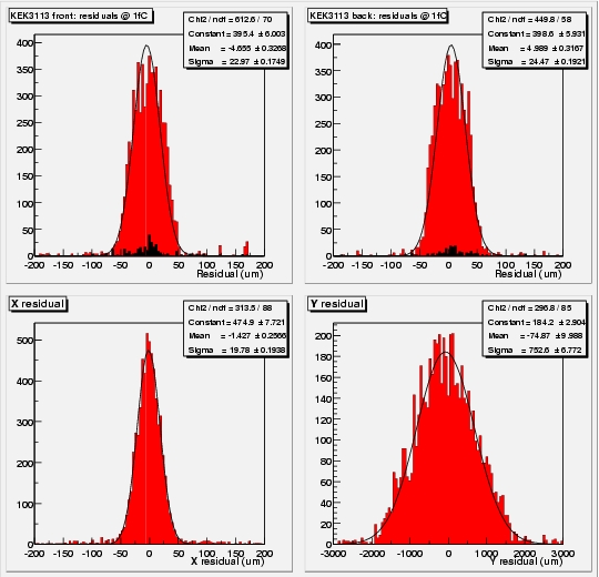
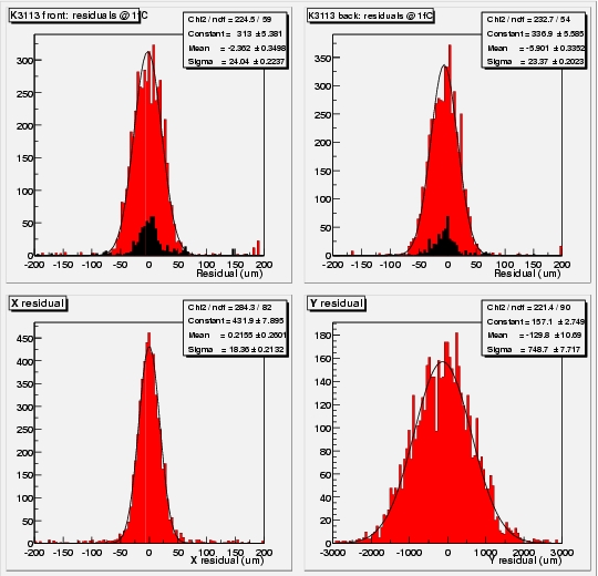
The spatial resolution is determined by plotting the difference between the extrapolated track position and the center of the binary cluster. Combining the u and v measurements from the front and back planes of the module, one can reconstruct X,Y space (intersection) points. These can again be compared to the extrapolated track position. The plots below show residuals in u, v, x and y for all barrel modules. In the forward case, the reconstruction is slightly more tricky (as the strips are not parallel). This will soon be done.
Residuals in u,v,x and y for K3113 at 1 fC, 350 V, 1.56 T, 0 degree incidence (left) and -13.8 degree (right). The resolution improves slightly at non-perpendicular incidence, due to charge sharing (leading to clusters of 2 strips)
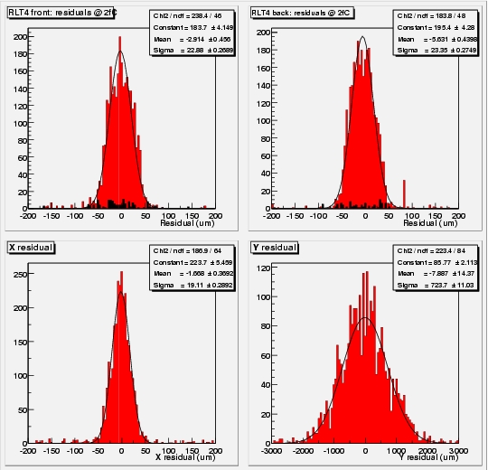
Residuals in u,v,x and y for RLT4 at 350 V, 1.56 T, 0 degree, 1.3 fC (left) and 2 fC (right). The resolution is worsened by the higher noise at "low" threshold. This could be a result of the rather primitive space point reconstruction.
The values found for the resolution more or less consistent among themselves. sx = su/Sqrt(2), sy = Sqrt(2) * su/a, where a is the stereo angle between the two planes.
The disappointing 18/19 microns in the x coordenate may be due to the extrapolation error becoming significant. Further investigation is needed.
Very few results are presented from forward modules,
although three of them were present. This is mostly because the noise
is much higher than on the barrel modules. It should be kept in mind
that the grounds were tied together on the hybrid and the support
card, but that there was no electrical contact between the cooling
block and the hybrid substrate. Also, the temperatures on the forward
hybrids went up to 40 or 50 degrees, while the barrel hybrids
remained at 10 degrees?
The multiplicity - number of hits per event - of
FRK153 from noise runs at 0.7 (upper left) and 1.0 fC (upper right)
and VAL1 at 1.0 fC (lower left)RLT5 (lower right). The result for
VAL1 was obtained from a normal beam run, as it was taken out before
the noise runs were taken.
The forward modules show a deviation from the
binomial distribution one would expect for random noise. The barrel
modules do not.
The S-curves discussed in the previous chapter allow
a determination of the median charge. Below, the median charge as a
function of bias voltage and incidence angle are shown for 0 and 1.56
T magnetic field and for an irradiated and non-irradiated barrel
module.
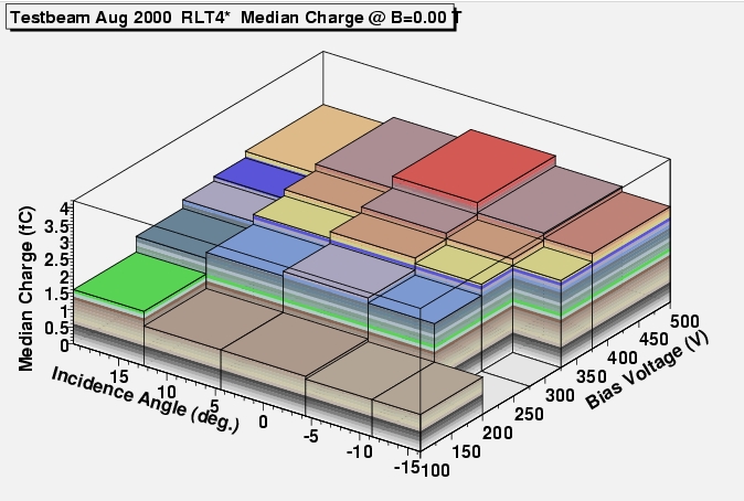
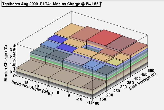
Median charge from an error function fit of the
S-curves for a range of detector bias voltages, incidence angles and
a magnetic field of 0 T (left) and 1.56 T (right). PostScript
for all modules
Median charge from an error function fit of the
S-curves for a range of detector bias voltages, incidence angles and
a magnetic field of 0 T (left) and 1.56 T (right). PostScript
for all modules
From the above plots, a couple of tendencies are
clear:
There is reasonable
agreement between both sides of all modules.
The median collected
charge is highest for perpendicular incidence in the 0 magnetic
field case.
The distributions get
asymmetric when the magnetic field is applied. The shift to negative
angles seams to be somewhere halfway 0 and -8.8 degrees (the central
value of the next to central bin) for both modules. The Lorentz
angle will be properly measured in the Lorenz angle section.
In the non-irradiated
module, a slight increase of the charge is seen with the detector
bias voltage. A quantitative treatment in the section on Ballistic
Deficit.
For the irradiated
module, the charge is a strong function of bias voltage that does
not reach a plateau in this range (up to 450 V).
(Only) At the highest bias voltage, the charge
collected in the irradiated module approaches the non-irradiated
case.
To get a more quantative feel for the tendencies of
charge with bias voltage the plot below shows the charge at perpendicular incidence, magnetic field on.
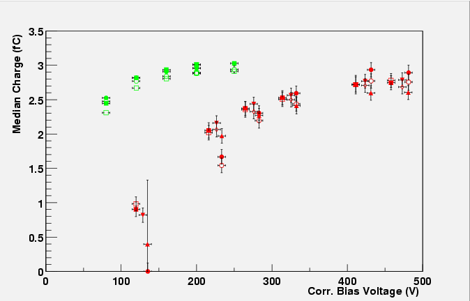
Median charge versus bias voltage, measured at
perpendicular incidence in a 1.56 T magnetic field. Non-irradiated modules K3112
(green circles), RLT5 (green squares), modules with irradiated
sensors K3113 (red circles), RLT9 (red triangles), RLT10 (red downward triangles) and fully irradiated module RLT4 (red squares). Front and
back plane of the module are drawn separately.PostScript
The median charge collected in the non-irradiated
modules was seen to decrease with bias voltage. Here, we will link it
to the pulse width produced by the shaper, which is a clear sign that
the charge loss is due to a ballistic deficit of the shaper.
In fact, the charge collection time for
non-irradiated p-on-n detectors of thickness d is approximately given
by:
T= d²/(µVbias) where mu is the mobility of the majority carriers.
Just above depletion voltage (80 V), one obtains 22.5 ns for thin
detectors, 29 ns for thick detectors. The shaper of the Front End has
a peaking time of 25 ns. Therefore, one would expect some amount of
charge to be lost due to ballistic deficit.
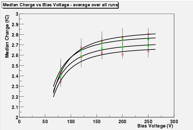
The median charge averaged over all angles and
magnetic fields for two planes of K3112 (green circles) and RLT5 (red
open circles). The charges in RLT5 have been scaled by (285/325) to
correct for the difference in thickness. Above depletion voltage the
charge is linear with d. The error bars indicate the variation in
charge due to angles and field, rather than a measurement error. Get PostScript
The charge as a function of bias voltage of the two
non-irradiated barrel modules is seen to be in good agreement after
rescaling RLT5's median charge. Both fit very well to a ballistic
deficit description where the charge is given by:
Q= Qtot (1 - 1/8*(d²/µ T Vbias)²)
where T is the ideal shaper peaking time and d the thickness of the Silicon wafer.
Filling in design values for the
thickness or shaper time and the theoretical value for the hole
mobility, one obtains a measurement of the remaining parameter. The
results for both modules are listed in the table. Module Full charge (fC) Shaper time (ns) Mobility (cm²/Vs) 90 % Voltage (V) K3112 front 2.8+/-0.1 22 400 90 K3112 back 2.7+/-0.1 22 400 85 RLT5 front 2.8+/-0.1 26 460 102 RLT5 back 2.7+/-0.2 25 460 103 As will be discussed in the section on irradiated
detectors, it is conceivable that a ballistic deficit occurs in the
irradiated detectors. This woud happen if the mobility decreases more
than the higher voltage can compensate for. There is no way to tell
what is the dominant effect directly from the charge vs bias voltage
plots. But additional information on timing can be obtained by
measuring the width of the efficiency versus TDC distribution
(combined for three time bins).
Width of the efficiency versus TDC distribution at
1 fC, averaged over all angles and magnetic fields. The unirradiated
modules (K3112 - green circles - and RLT5 - green squares) show a
clear increase at low voltages. The modules with irradiated sensors
K3113(circles), RLT9(red triangles) and RLT10(red squares) show
clearly narrower distributions. RLT4 (black squares) on the other
hand has a very wide distribution, especially on the back (open
squares). The time walk had already been measured to be very
different between both sides (17.7 ns on the front, 13 ns on the
back, see also
http://eklund.home.cern.ch/eklund/IrradHome.htm)PostScript,
PostScript of all modules individual distributions
The narrow TDC distributions in the modules with
irradiated sensors indicate there is no ballistic deficit at voltages
from 250 V upwards. The wide distribution is caused by the increased
shaper time due to the irradiation of the Front End electronics. Both
sides of the module were measured by Lars Eklund to have very
different timing characteristics (see also
http://eklund.home.cern.ch/eklund/IrradHome.htm). However, one would
expect the side with the lower time walk also to have the narrower
distribution. Here, it is the other way around.
After irradiation to the full dose expected for ATLAS
(3*1014 protons), the depletion voltage of the detectors should settle around 250 to 300 V.(can anyone tell whether this number is approximately correct? What values were measured on these detectors?) The bulk has inverted type. The mobility of the majority carriers
may change by an unknown amount. And lattice defects trap a certain
amount of the charge (that depends on the carrier velocity and thus the bias voltage). A combination of these effects leads to the
median charge vs bias voltage curves below.
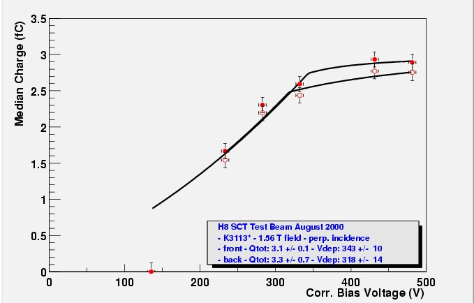
The corrected median collected charge - from runs at perpendicular incidence and in a 1.56 T magnetic field - as a function of corrected bias voltage. The charges have been recalibrated and scaled with sensor thickness, whereas the bias voltage is corrected for the voltage drop in the bias resistors. PostScript files 1234
In the ballistic deficit chapter, the conclusion was that no evidence for ballistic deficit could be found for the irradiated modules. This means the fit used for the non-irradiated detectors would not return very usefull results (although it does fit). Instead, the median charge vs bias for the irradiated detectors will be fit to a model by G. Casse and S Marti i Garcia [See for a thorough description: Charge collection for irradiated p+n detectors]. Below the full depletion voltage the sensors are partially depleted:
w(V) = w0 Sqrt(V/Vdep).
Charge trapping in the depleted region due to lattice defects is taken into account by supposing the carriers in the depleted region to have a mean free path given by:
l(x) = l0 + l1 * E(x)/Es
,whenever E(x) is below the saturation field. Module Side Charge (fC) Depletion (V) l0 l1 saturation field K3113 front 3.1 +/- 0.1 343 +/- 10 150* 2400* 0.5 +/- 3 K3113 back 3.3 +/- 0.6 318 +/- 14 150* 2400* 0.6 +/- 3 RLT4 front 3.3 +/- 0.5 243 +/- 12 150* 1400 1.5 +/- 3 RLT4 back 3.6 +/- 0.6 244 +/- 13 150* 1200 2.0 +/- 3 RLT9 front 3.3 +/- 0.8 258 +/- 14 150* 1200 1.8 +/- 1 RLT10 front 3.2 +/- 0.3 253 +/- 12 150* 1700 1.2 +/- 4 RLT10 back 3.5 +/- 0.8 247 +/- 13 150* 1200 1.9 +/- 1.6 Median charge fit results for all modules with irradiated sensors.
The l0 was bounded to be within one sigma of the value found by G. Casse and S Marti i Garcia. l1 and Es are left to vary, but the obtained values are not significant as a measurement. The asymptotic charge is in reasonable agreement with the results with the unirradiated modules. Then, good agreement is found for the full depletion voltages of both sides of the modules. K3113 has a surprisingly high value, which is mostly due to it not being efficient at all at the lowest bias voltage. RLT4 has thicker detectors and would be expected to reach full depletion at a higher voltage. Experts??
As mentioned, the depletion voltage of the irradiated
sensors should be somewhere between 200 and 350 V. After type
inversion the junction is on the n+ side (backplane). If the detector
is not fully depleted, the signal is induced on the strips by the
moving charges on the back of the detectors. The spatial structure of
the signal may be very different from that resulting from diffusion
in the fully depleted detector. Here, we will study the average
cluster width of the efficient clusters. In case the charge is shared
between strips (more than in the fully depleted case, this will have
a negative effect on the efficiency.
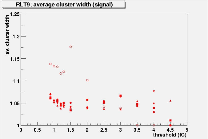
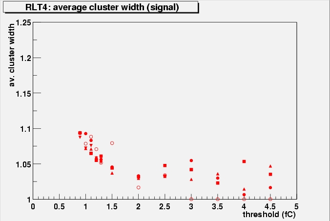
The average cluster width of clusters close to the
track as a a function of threshold for different bias voltages. Open
circles correspond to the lowest voltage (150 V), closed circles to
250 V, squares to 300 V, triangles to 350 V and 450 V. The first plot
is of the unirradiated Valencia module, which should give an idea of
the behaviour in unirradiated, depleted detectors. Only perpendicular
incidence, no field data have been used, but other scans show similar
behaviour. Get all PostScript files
The figures show a clear increase in the average
cluster width in the 150 V data, indication of the above described
effect. For 250 V the effect - if at all there - is reduced to within
the error bars. RLT4 seems to insensitive. This means it will not
limit operation ranges, as at 150 V the modules were not expected to
collect enough charge, even without this effect.
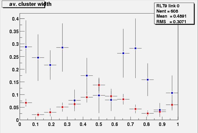
A more detailed way to look at this is to plot the
average cluster width as a function of the interstrip position of the
track:
The average cluster width (the offset of 1 has
been subtracted) of the clusters caused by signal for two runs at
0.89 fC, 1.56 T field, perpendicular incidence at 150 V (blue) and
500 V (red) detector bias.
The increase of the cluster width in a narrow region
between two strips (interstrip position 0.5) - typical for spatial
distribution dominated by diffusion of the charge carriers - is clear
in the 500 V data, but seems not to be present in the 150 V data.
Unfortunately, statistics are very low for the 150 V runs, as the
modules are only 10-20% efficient. (care has been taken to select
runs that share the same alignment, are close together in time and at
perpendicular incidence. These requirements could not be fulfilled
for magnet off data, therefore magnet on runs had to be chosen).
Lorentz Angle
The magnetic field causes the holes travelling toward
the strips to be deviated and follow a path that is at a fixed angle
irrespective of the electrical field. This angle is called the
Lorentz angle. For a 1.56 T field on p-on-n Silicon we expect this
angle to be 2.7 degrees. It can be measured by varying the angle of
incidence of the beam and find the minimum in the average cluster
width due to signal. That is the point where least charge sharing
occurs, ie where the incidence angle cancels the Lorentz angle.
Average cluster width of the efficient cluster as
a function of incidence angle in a field of 1.56 T for a number of
thresholds. The minimum (least charge sharing) is clearly shifted to
small negative angles at all thresholds.
The Lorentz angle will be taken to be the average of
the minima of 4 parabolic fits to thresholds of 0.9, 1, 1.2 and 1.3
fC. Now, one can plot the Lorentz angle measured at different bias
voltages.
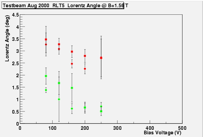
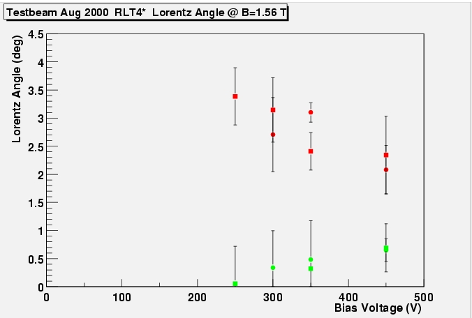
The Lorentz angle as a function of detector bias
voltage for an unirradiated (left) and an irradiated (right) module.
The green points correspond to measurements done without magnetic
field and somehow define 0. The red points are from runs with 1.56 T
magnetic field. One would expect a constant Lorentz angle at 2.7
degrees. PostScript files for all modules
The Lorentz angle as a function of detector bias
voltage for an unirradiated (left) and an irradiated (right) module.
The green points correspond to measurements done without magnetic
field and somehow define 0. The red points are from runs with 1.56 T
magnetic field. One would expect a constant Lorentz angle at 2.7
degrees.
The figures above seem to find a decreasing Lorentz
angle with bias voltage. However, the spread in points is again quite
big and things do not become quite significant. The figures below
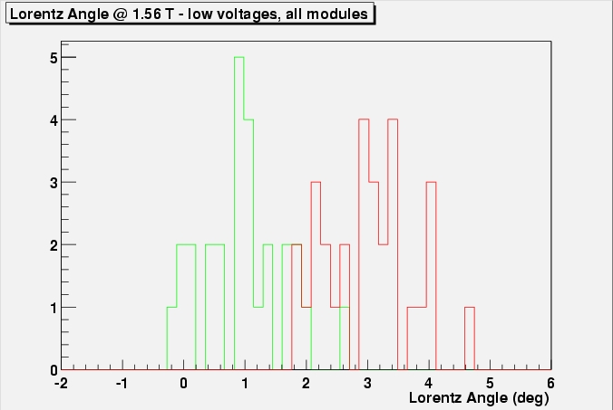
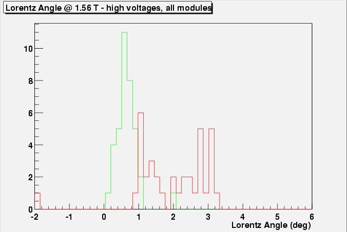
histogram all Lorentz angles found in all modules in either of the
two histograms, low voltages (80 and 120 unirr., 150, 250 irr.) in
the left one, high voltages in the histogram on the right (200 and
250 unirr., 350 and 450 on the right).
Lorentz angles of all modules histogrammed for the
low voltage runs (left) and high voltage runs (right). The green
histogram corresponds to values obtained at 0 field, the red one to
1.56 T.
With the spread in the measurements shown before, one
can simply not believe there is a dependence on bias voltage. The
final Lorentz angle would then look like:
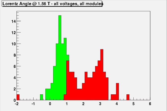
Lorentz angles of all
modules histogrammed. The green histogram corresponds to values
obtained at 0 field, the red one to 1.56 T.
Charge vs Angle
In the experiment, tracks will fall on to the sensors with varying angle, depending on the track momentum, the radius of the Silicon layer, etc (the angle referred to is the angle in the direction perpendicular to the strips, leading to charge sharing). The charge and efficiency were seen to depend on an the incidence angle. The variation of charge with incidence angle is fitted with a parabola.
The median charge as a function of incidence angle in a 1.56 T magnetic field and at various bias voltages. PostScript files
The fit values measure the Lorentz angle (which is again seen to decrease with voltage), but can also be used to derive a number indicating the sensibility of the charge to incidence angle. For all these modules and all voltages except the lowest, the angle where the charge had decreased to 90 % of the maximum value (of that particular module at that bias voltage) was found to be 14 degrees +/- 1 in the magnetic field and 12 degrees +/- 1 without field.
These conclusions are not the result of an extensive discussion among experts, but may hope to provoke such a discussion.
 <
<

Forward modules


Median Charge


Ballistic Deficit

Irradiated detectors


Underdepleted operation


Angles


Conclusions
![]() Last
update November 10, 2000
Last
update November 10, 2000
Marcel.Vos@ific.uv.es,