| Source | Nycomed Amersham SIR 1211 sealed Strontium-90 source |
| Triggers | Scintillator material read out by Hamamatsu H6780 PMTs |
| NIM modules | LRS 620 CL 8 channel discriminator |
| LRS 688 AL TTL-NIM-TTL translator | |
| CAEN 4 channel discriminator | |
| CAEN 92 NIM-ECL-NIM translator | |
| CERN NP N 2251 timinig unit | |
| CERN NP N6237 coincidence | |
| CERN NP N4149 logical fan-out | |
| CERN NP N9053 delays (0-63 ns) | |
| CAEN N126 HV source | |
| VME | Bit 3 crate control interface |
| interface to CAMAC | |
| UCI VME/DSP/LL/TCC cards | |
| Bias card 96 | |
| Bias card | |
| CAMAC | LeCroy 2249 A 12 channel TDC |
| LeCroy 2228 A 8 channel ADC | |
| Clock | Philips PM 5786 pulse generator |
| Delay | Stanford delay |
| High Voltage | Keithley K236/K237 |
| X-Y stages | Newport UTM stages and MM4005 controller |
Radioactive source: Strontium 90
Decay mode: Sr90->Y90
+ 0.546 MeV e
Secondary:
Y90-> Zr90 + 2.283 MeV e (99.98%)
Life time Sr:
28.6 years
Life time Y:
64.1 hours
Intensity:
46.2 kBq. (factory specification)
Radius:
250 mm
Thickness:
50 mm
Radiation:
Betas in the [0-5] MeV range
The source produces electrons with energies in the 0.5 to 3 MeV range,
a bit too low to leave a genuine MIP signal in the silicon. Typically,
the signal left is slightly larger and has a wider distribution than higher
energy particles (as expected in ATLAS). A calculation of the charges deposited
in 300 um of silicon is shown here.
This source, in the present setup, yields 25000 triggers in AND mode
in about 10 hours. After cutting on the TDC value, roughly 15000 remain,
enough to fully characterize a module.
For parameter optimisation runs, where a large number of counts is
more important than noise rejection, one can obtain a factor 10 more triggers
by running in OR mode.
A second Strontium source is available with the same energy characteristics
but a factor thousand more intense.
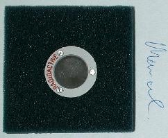
The photo shows the low intensity source in its encapsulation, next
to normal size handwriting.
Triggers: readout of the silicon detectors is triggered by two scintillator
detectors
10 by 10 by 4 mm scintillators, read out by Hamamatsu H6780 photosensor
modules.
PMT specifications:
Dark current
0.5/10
Anode pulse rise time 0.65 ns
Radiant sensitivity
21
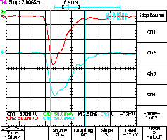
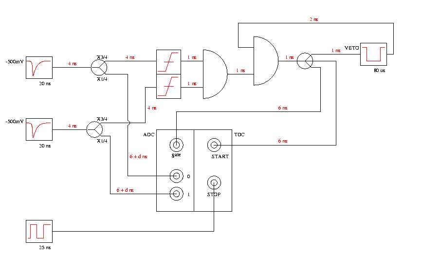
The sensitive parts are aligned so as to overlap. Typical pulse shapes can be seen in the oscilloscope screenshot below. The squares correspond to 2.50 ns (x-axis) and 50 mV (y-axis). The blue pulse corresponds to the detector nearest to the source.
At the nominal voltage (800 V) and a discriminating threshold of -100
mV, excellent noise rejection (noise level <1/10000) can be achieved,
forming the logical AND of both discriminated pulses. The details of trigger
preprocessing can be seen here.
The resulting logical TTL trigger pulse is sent to the TDC and converted
to a 60 ns ECL pulse, which is input to the TCC trigger line.
TDC: information on the phase of the trigger with respect to the 40
MHz system clock is saved, in order to be able to reject inherently less
efficient events (where the signal is largely outside the time bucket)
LeCroy 2249 12 channel TDC
range:
100 ns (200 and 500 ns settable by dipswitch)
resolution:
50 ps (100 and 250 ps)
dead time:
7 ns
digitisation time: ~1 us (can be lowered by not considering
all 10 bits)
Times are determined up to 50 ps resolution in the 100 ns range for
normal data taking. Longer time scales are available, with lower resolution.
These are used only for scans over the TCC delay.
The time information of interest is the phase of the raw trigger, with
respect to the 40 MHz, randomly distributed in the range from 0 to 25 ns.
In order to avoid the ~7 ns dead time of the TDC, the actual time we measure
is the difference between the raw trigger, delayed by a settable amount,
and the synchronised trigger, as it is output by the SLL card. This method
allows us to measure the 25 ns period of interest with a fixed offset (of
say 25 ns) and thus avoid the dead time.
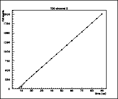
The TDC was calibrated using the Stanford delay generator,
showing an excellent linearity (error less than 1 count) in the range from
20-90 ns.
Delay generator: the delay of the raw trigger signal is generated by
a Stanford.
Resolution: 50 ps
Range: up to microseconds
Clock: the 40 MHz external clock is generated by a Philips PM5786 pulse
generator
Frequency range: 1 Hz -125 MHz
Risetime
: 2 ns
An important feature is the adjustable duty cycle, as the pulse changes
characteristics on being converted from TTL to NIM and NIM to ECL.
Irvine DSP/SLL/TCC VME modules: The readout and control of the module
uses DSP, SLL and TCC cards, developed by the University of Irvine. More
information can be found on their webpages:
http://positron.ps.uci.edu/~pier,
for example.
High Voltage sources: The detectors under test are biased using a CAEN
N 126 NIM module HV source. It can provide up to 3mA for [0-3kV] with a
settable safety maximum on the current delivered. For precision tests,
a Keithley K236 source/measurement unit is available (normally used in
the detector
characterisation setup).
Protective cage: A large hermetic Faraday cage shields the setup, consisting
of the module, the source and the triggers, including a small HV unit for
the PMs, both from light (which would leave a signal in the biased detectors)
and electromagnetic noise. Special care has been taken to make the cage
fully conductive.
X-Y stages: The X-Y stages are Newport UTM---150 and UTM---100, covering
the full sensitive area of the module. The MM4005 controller has a GPIB
interface and can thus be controlled from the PC. Position accuracy is
1 micron, for laser test purposes.