|

Optical Multiplexer Board 9U
Introduction
TileCal is the
hadronic tile calorimeter of the ATLAS-LHC experiment and consists in terms
of electronic readout of roughly 10000 channels read each 25 ns. Data
gathered from these channels are digitized and transmitted to the Data
Acquisition System (DAQ) following a three level trigger system (Fig.1).

Fig.
1.
The ATLAS three levels trigger
system.
The main component of the back-end
electronics of the TileCal sub-detector is the Read-Out Driver (ROD) which
is placed between the first and the second level trigger. The ROD has to
pre-process and gather data coming from the Front End Boards (FEB) and send
these data to the Read-Out Buffers (ROB) in the second level trigger.
TileCal electronics will receive about
2 Gy/year (0.2 Krad/year)
of radiation for a total dose of 20 Gy in the
experiment lifetime To measure
radiation hardness of TileCal FrontEnd
electronics, tests were conducted with proton beams in different areas and with
different beam sizes. Thanks to these tests, three non-destructive kinds of
errors were found:
·
Transient error in the data flow out to the ROD.
·
Permanent errors in the data flow requiring reset.
·
Latch-up error with an increment in current consumption of 60 mA.
To reduce data
loss due to radiation effects, the TileCal collaboration decided to include
data redundancy in the output links of the FrontEnd.
This was accomplished using two optical fibres which transmit the same
data. At ROD system level, data redundancy is used to discard the fibre
with errors due to radiation. The checking is based on rightness of the
Cyclic Redundancy Codes (CRC) of the data packets on both fibres. This is
also necessary as the ROD motherboard is expecting just one fibre per
channel. For this purpose a new module, called PreROD
or Optical Multiplexer Board (OMB) was conceived (Fig. 2). This board would be able to provide, in case of error in
one link, the correct data to the ROD input by analyzing the Cyclic
Redundancy Codes (CRC) of the data packets on both fibers coming from the
FEB.

Fig. 2.
The OMB in
the TileCal data acquisition chain.
THE OMB 9U FINAL
PROTOTYPE
The final OMB 9U prototype (Fig. 6) is
designed from the 6U board experience. This prototype is conceived in a 1
to 1 ratio with respect to the RODs, i.e. each board has 16 input links and
8 output links, setting the final format in a 9U VME standard board.
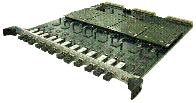
Fig.
3.
Picture of the OMB 9U prototype
board.
From the functionality point of view
there are some minor modifications being the most important, the inclusion
of the TTC receiver chip. This would lead to the possibility receiving the
trigger directly from the TTC system. In view of future upgrades and to
increase the functionality the design includes four PMC connectors for
mezzanine boards connected to the CRC FPGAs and is designed for 80 MHz
operating frequency instead of the nominal 40 MHz of the LHC. This last
issue poses some problems related to signal integrity and component
placement aspects. Among them, the use of a single JTAG chain for the
programming of all the FPGA chips in the board, the bus connecting the VME
controller and the CRC controllers and the clock distribution are the main
concerns.
The PCB Specifications
The OMB final prototype layout is a 10
layer PCB which optimize the cross-section to
minimize signal integrity problems. Fig. 7 shows the arrangement of the
layers. We tried to keep every signal layer between two power planes or,
when it was not possible, routing the two adjacent layers orthogonally.

Fig.
4.
OMB 9U prototype layer stackup.
The power distribution is also a
concern in this board as we must supply several voltages. All the FPGAs
need 3.3 V for the I/O and 1.5 V for the internal operations. The NIM to
TTL conversion for the external trigger signals needs a 12V supplied
voltage while other logic circuitry needs 5 V. The 12 V and 5 V power
supplies are taken from VME bus or, when it is not available or for
testing, from special pins on the board. The generation of the lower
voltages (3.3 V and 1.5 V) is accomplish by voltage regulation from the 5 V
main power supply. With this configuration, the power plane in layer number
2 is connected entirely to 3.3 V whereas the power plane in layer number 9 is
a split plane with 1.5 islands below the FPGAs (Fig. 8).

Fig.
5.
Power distribution in the internal
layer number 9.
Components
Fig. 6 shows the top layer layout with
the main components highlighted. In the OMB 9U board there are more than
1200 components connected with more than 2000 nets. The components
distribution is not uniform and they are mainly placed near the front-panel
since these components are used to process or to inject data through the
optical connector placed in the front-panel. The mezzanine connectors for
the daughterboard cards are mounted in the center of the board. Finally,
the VME interface and the TTC receiver are placed close to the VME
connectors.
The Optical Connectors
Stratos Lightwave dual optical
receiver (M2R-25-4-1-TL) and transmitter (M2T-25-4-1-L) are chosen to
optimize the space in the board. Since 16 inputs and 8 output links are
needed there are 8 dual receivers and 4 dual transmitters in each board.
The dual receiver connectors receive an optical fiber from the front-end
and transform it into a electrical PECL
differential signal whereas the dual transmitter connectors transmit the
differential signal to the optical fiber. These differential lines, which
connect the optical connectors and the G-Link chips, were manually routed
and their impedance controlled, because these lines transmit high speed
signals (640 Mbps).
The G-Link Chips
The G-Link chips serialize (HDMP-1032)
and de-serialize (HDMP-1034) the data transmitted and received through the
optical connectors. The HDMP-1034 receiver chip receives the differential
signal directly from the optical receiver and transforms it into a 16-bits
bus. These chips are individually clocked with a 40 MHz oscillator placed
close to the chip. Moreover, the HDMP-1032 transmitter chip receives the
16-bits bus from the CRC-FPGA and transforms it into a PECL differential
bus. These chips are also clocked at 40 MHz but this clock is generated
internally by the FPGA firmware. There are in total 16 receiver chips and 8
transmitters.
The CRC-FPGA
The CRC-FPGA is the main component of
the OMB 9U because they are responsible for the data checking in the CRC
operation mode and the generation of data in the injection mode. There are
8 CRC-FPGAs in each board and they are ALTERA EP1C12 devices, also used in
the previous 6U prototype design. These devices will receive directly the
front-end data for the CRC checking. Nevertheless, it is possible to
include more functionalities as a Bunch Crossing Identification (BCID)
checking, because these devices will receive through the TTCrx chip all the TTC information generated by the
Central Trigger Processor (CTP). All the error counters as well as the
configuration and status registers are also included in the CRC-FPGAs
firmware and they are readable and/or writable through the VME bus.
Besides, the CRC-FPGAs are connected
to the Processing Units (PU) connectors for future upgrades. In this case,
the data received in the CRC-FPGA might be sent to the PU for processing
tasks before its transmission to the RODs.
Finally, the CRC-FPGAs firmware is
downloaded by using the JTAG chain or in a Passive Serial mode by using the
Erasable Programmable Read-Only
Memory (EPROM) memories mounted in the board, there are two EPROM
for each 4 CRC-FPGAs.

Fig.
6.
The OMB 9U prototype main components.
The VME Interface
The interface with the VME bus is
managed by the VME-FPGA, which is implemented in a CYCLONE EP1C20 device.
The VME-FPGA generates the geographical address of the board and represents
the interface between the VME bus and the CRC-FPGAs in order to read and/or
write the registers physically placed in the CRC-FPGAs. It provides also
the VME communication with the TTC-FPGA. Besides, the VME-FPGA might be
used to internally generate a trigger signal in the injection mode.
The TTC Interface
The TTC interface is implemented in
the OMB 9U with a TTC receiver chip (TTCrx) and
the TTC-FPGA. The TTC information is received in the TTCrx
through the backplane and it includes the Bunch Crossing (40 MHz), the
Bunch Crossing Reset (BCR), the Level 1 Accept (L1A), the Event Counter
Reset (ECR) and the Trigger Type (TType). With
these signals, the TTC-FPGA generates the Bunch Crossing Identification
(BCID) and the Event Identification (EVID). These signals and the TType are transmitted to each CRC-FPGA with each L1A
received.
The TTC information might be used in
the OMB 9U board to check the BCID of the data received from the Front-End
or to inject data to the ROD with actual TTC information.
Operation Modes
The CRC Checking
In the CRC checking operation mode the
OMB 9U receives 16 fibers from 8 Optical Interface Boards (OIB) and
transmits 8 fibers to one ROD (Fig. 7). Each CRC-FPGA must check the CRC of
two redundant inputs and decide which one is transmitted to the ROD system.
Moreover, the decision has to be taken in real time but a latency time is
introduced in the acquisition chain. The algorithm that decides which fiber
is transmitted and which is discarded consists of two simultaneous
operations. The events received through each input link are stored in two
different memories while the CRC is computed. The last word of the event
includes the global CRC computed in the Front-End over the entire event.
When this word is received the algorithm checks the CRC and decides which
memory output is enabled.

Fig.
7.
Dataflow of the OMB 9U prototype CRC
checking operation mode.
Apart of the global CRC, it is
possible to decide which fiber is transmitted to the ROD system by checking
the DMU CRC (included in the trailer) or the BCID (included in the header)
of each DMU data block (16 per event). All the errors detected are counted
and stored in the corresponding internal register.
The Injection Mode
There are two different injection
modes as described above for the previous 6U board: the counter and the
memory injection modes. The main differences with the previous 6U version
are the number of output channels and the possibility of the injection of
data with actual TTC information. With a OMB 9U it
is possible to inject data to a whole ROD through its 8 optical outputs
(Fig. 8). Furthermore, the TTC feature permits the injection of data with
the TTC information received through the backplane. Since this information
is also received in the ROD, it is possible to test the TTC synchronization
at ROD level with the data generated in the OMB 9U.
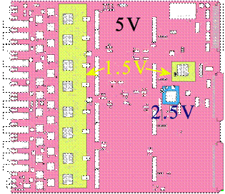
Fig.
8.
Dataflow of the OMB 9U prototype
injection mode.
The
complete design including schematics and PCB artwork is available in the
CERN EDMS web page. (EDA-01518-V1-0)
|