L. Eklund
CERN
K. Hara
Y. Kato
H. Kobayashi
S. Shinma
Tsukuba University, Japan
Y. Ikegama
T. Kohriki
T. Kondo
S. Terada
N. Ujiie
Y. Unno
KEK, Tsukuba, Japan
Y. Iwata
H. Masuda
K. Yamanaka
Hiroshima University, Japan
C. Ketterer
Freiburg University, Germany
G. Moorhead
University of Melbourne
R. Takashima
Kyoto University of Education, Japan
J. Bernabeu
J.E. Garcia
C. Lacasta
G. Llosa
M. Vos
IFIC - University of Valencia
This page summarizes the Valencia analysis of the SCT beam test at KEK in December 2000.
Since the February SCT week, a lot of new information has become available about the temperature dependence of ABCD3T's DACs. This will lead to a recalibration of the forward with respect to the barrel modules (the forward hybrids were typically 35 degrees hotter). At least part of the median charge difference can be explained as a temperature effect of the CalDAC. The measurements can be found on the electronics page
June 28, 2001: The analysis is (hopefully) finalised. The results have been corrected for the temperature and irradiation dependence of the calibration DACs, the real value of the calibration capacitance. (The correction for the irradiation - a 3% decrease in DAC output - is based on the measurement of one chip). The new results are available as Encapsulated PostScript files in this directory.
Presentation in the February 2001 SCT week.
In December a week of beam was available is KEK's proton synchrotron. Submitted were 6 modules and 1 binary reference, three pairs of analog modules (used as a telescope). The DUTs were:
A series of threshold scans was taken at different bias voltages in two periods: during run I all modules were run with shaper bias 30 uA, while run II has the irradiated modules at a shaper bias of 24 uA. The front end bias current was 220 uA in all modules. The bulk of the data was taken in run II. Incidence angle was perpendicular, no magnetic field is present.
The three pairs of telescope planes are interspersed with the binary modules. They have excellent efficiency and allow for the reconstruction of a good, single track in 70% of the events. The rejected tracks include those that have kinks due to multiple scattering (remember these are 4 GeV protons). Only in the outermost modules a slight worsening of the reconstruction precision occurs. There should be no effect on the efficiency or noise measurements.
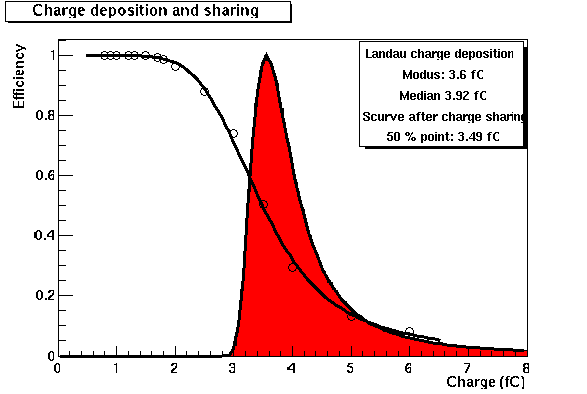
There is a rather large difference between the median charges obtained in August in H8, when compared to the ones presented here. Also, the forward modules seem to retrieve more charge than the barrel. In order to know what charges one would expect, the theoretical Landau charge deposition distribution is drawn in the figure below. The median charge is 3.92 fC. Then, one can simulate the contribution from Gaussian noise (1500 ENC) and the effect of charge sharing between strips. The resulting S-curve is drawn in the same figure. The combinationof noise and charge sharing has lead to a reduction of the median charge to around 3.5 fC (at perpendicular incidence).
The efficiency and noise occupancy have been determined for run II. Efficiency is measured in the central time bin (LEVEL compression) in a 12 ns wide fixed TDC interval (optimised for each module). The spatial acceptance is 100 um, events with a track pointing to a bad channel or its inmediate neighbours are rejected. Noise are those hits that are further than 1 mm from the track and not in a bad channel or inmediate neighbour. The noise occupancy is given per time bin (LEVEL compression). The TDC interval is quite wide, in order not to loose too much statistics. This will affect the efficiency when the pulse becomes very narrow, i.e. at high threshold, resulting in an apparently lower median charge. Also, the comparison between modules with different shaper times will not be valid. An attempt to get around this by reconstructing the entire pulse shape is described below.
Meanwhile, the results of the conventional analysis are available below.
A preliminary summary ntuple of all runs in run II.
PostScript files of some of the Scurves from run II. The naming convention is [module name]_scurves.ps. Modules are numbered 1 through 6 in the order of the above list.
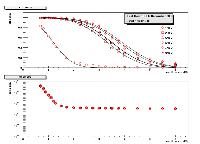
As an example the Scurve and noise occupancy for various bias voltages are shown below for the Valencia irradiated module. The high tail in noise occupancy must be due to a noisy channel. It does not appear in any of the other modules, nor in the second link of this module.
The idea is to plot the efficiency as a function of threshold and trigger phase (the generalised one, that combines the three time bins). This gives the plot below.

From left to right the efficiency decreases with threshold. Going up along the trigger phase axis one can recognise the shaper pulse. The color of 50% efficiency was changed to red to make it more visible. The shaper pulse is now extracted from the above plot by fitting the Scurve of each 1 ns trigger phase interval and plotting the median charge as a function of trigger phase (time). The resulting pulse shapes for various detector bias voltages are shown below for an unirradiated barrel module and an irradiated forward module.
Reconstructed shaper pulse for an unirradiated barrel module.

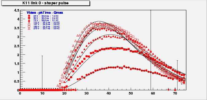
Reconstructed shaper pulse for VAL166, an irradiated forward module.
Note that the input charge in the test beam is varying randomly in a broad range. Laboratory measurements using the calibration circuit are necessarily different. They offer the advantage of one extra controlled parameter. Here, we try to reconstruct the pulse in circumstances as similar as possible to the final experiment.
The maximum charge of the reconstructed pulse can be compared to the Scurves shown before. The 50 % efficiency point in the S-curves above coincides with the average over 12 ns around the optimum TDC value, whereas ideally it should be exactly the peak value. Here, we see the difference is limited to the order of 10ths of a fC.
In nearly all pulse shapes a deviation from CRRC shape - a shoulder - is observed. This is probably due to the fact that we measure the response of the shaper to a broad distribution of input charges (Landau, smeared by charge sharing). The shoulder might correspond to charges close to the discrimination threshold that time walk to give a late hit. The fit allows the variation of peak charge, peaking time and an offset in time, but fixes the charge offset to 0 (that is: it trusts the calibration) and the order of the CRRC circuit to 3.
The plotted charges were obtained from a CRRC3 response function fit to the reconstructed shaper.

The median charge versus bias voltage. In green the average of the unirradiated barrel modules, in blue the unirradiated forward modules. Red circles: the irradiated barrel module K3. Red crosses: the irradiated forward module VAL166. The bias voltage is the supply voltage. In the irradiated modules - due to the high leakage current - there is a voltage drop of up to 40 Volts in the bias resistor.
In the unirradiated modules, charge is lost due to ballistic deficit from around 150 V. Below the depletion voltage the charge drops off linearly with bias voltage.
For irradiated modules below the depletion voltage, the charge increases linearly with bias voltage (see for example by L.J. Beattie et al, The electric field in irradiated silicon detectors, NIM-A 418(1998) 314-321) The kink where the charge stops rising linearly is around 300 Volts for both modules. We will take this number as the best measurement of the depletion voltage available at this point. Above the depletion voltage the charge keeps on rising slowly all the way up to 500 V.
Above the depletion voltage, model calculations and measurements have been done of the charge collection time as a function of bias voltage (see for example: Brodbeck et. al., Carrier mobilities in irradiated silicon, 5th conference on position sensitive detectors, London. Available as ROSE/TN/2000-09). The figure below presents a calculation of the charge collection based on the model and measured mobility and saturation velocity of Brodbeck et al for a non-irradiated 285 micron thick detector and the same detector after 2.4 E14 n/cm2. The depletion voltage of the irradiated detector was set to 300 V, as no measurements are available.

Expected charge collection times.
In the non-irradiated case, the collection time becomes "large" - more than 10 ns - around 150 Volts. This coincides with the on-set of the ballistic deficit. In the irradiated modules a similar "large" collection time would be expected between the depletion voltage (set to 300 V) and maybe 50 V overdepletion. Thus, we might expect some evidence of ballistic deficit in this region.
Below the depletion voltage the non-depleted region prevents the holes to reach the strips (at least in the irradiated case). However, a signal is induced in the strips. The time constant of this effect is not clear to me at this point. Suggestions are welcome.
The pulse shape reconstruction allows a study of the effect of the bias voltage on the shaper pulse length. In some cases, this may be used to infer the properties of the detector pulse. In the future, a detailed simulation of the response of the shaper to different pulses will quantify the current argument. The figure below present the effective SHAPER peaking time obtained from a CRRC3 fit of the reconstructed shaper pulse. The error bars on the points are a measure of the variation between different modules and link 0 and 1. A detailed study of the fit quality and error estimation are to be done.
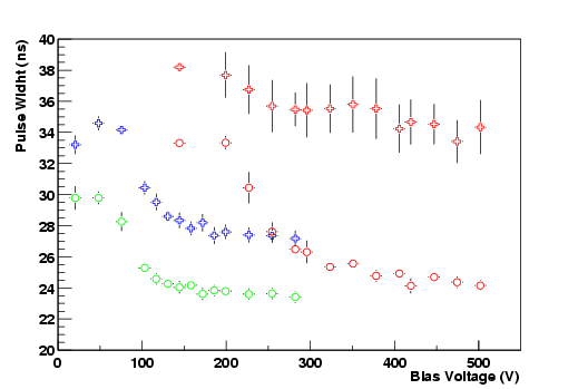
The shaper pulse peaking time versus bias voltage. Again, in green the average of the unirradiated barrel modules, in blue the unirradiated forward modules. Red circles: the irradiated barrel module K3. Red crosses: the irradiated forward module VAL166. The bias voltage is the supply voltage. In the irradiated modules - due to the high leakage current - there is a voltage drop of up to 40 Volts in the bias resistor. The error bars represent the variation between modules and/or links.
In the unirradiated modules the ballistic deficit is clearly visible in the gradual rise of the pulse length when decreasing the voltage from 150 to 80 V. Below the bias voltage, a strong rise in the peaking time is observed. Only the lowest bias voltage shows a lower pulse length. The barrel modules seem to be faster than the forward modules.
For K3, the irradiated barrel module, the pulse length is slightly larger than for the unirradiated modules at the same voltage. Below the depletion voltage, a quite steep rise is observed. The irradiated forward module - VAL166 - shows a very long pulse, with a quite large difference between both links (causing the large error bars).
The resolution in silicon strip detectors with binary read-out is, given the strip pitch, determined by the number of strips in the cluster. The plots below show the average cluster size for efficient clusters. That means that only clusters that have their center within 100 microns of the extrapolated enter in the average.
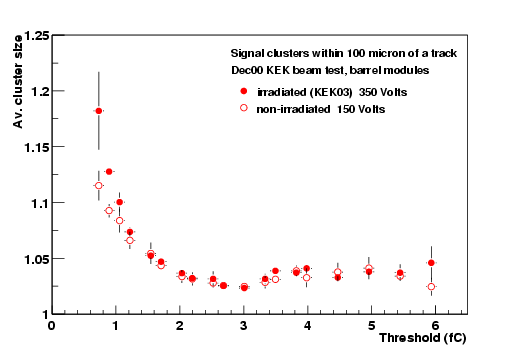
Average cluster size of efficient clusters as a function of discriminating threshold. Shown are an irradiated and non-irradiated barrel modules at nominal detector bias voltage. The increase in cluster size at low threshold is more pronounced in the irradiated module (reflecting the fact that it is noisier? or maybe an increase in cross-talk? interstrip capacitance?)

The dependence of cluster size on bias voltage is very moderate for the non-irradiated modules. The decrease below depletion voltage is due to the loss of charge collection. Raising the voltage from around 150 Volts to 275 Volts leads to a slight decrease of the average cluster size. In a high field the charge is collected faster and the effect of diffusion is less important. The irradiated module is a bit more complicated. The slight decrease from 350 to 500 Volts can be attributed to the collection time - diffusion effect. Note, that the plateau value is very similar between the irradiated and non-irradiated modules, although at very different voltages. Then, around the depletion voltage, the cluster size rises dramatically. The explanation might be that the strips are not very well isolated from each other in a type-inverted, under-depleted detector? Moreover, the signal has to be induced across a dead, non-depleted region, leading to a less localised signal? At even lower voltages, the signal becomes very small and reduces the average cluster width.
Below, I summarize some of the results so far.
![]() Last
update November 10, 2000
Last
update November 10, 2000
Marcel.Vos@ific.uv.es,Pepe.Bernabeu@ific.uv.es,